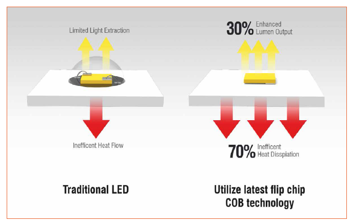
COB is already a mature technology in the electronics manufacturing industry, but general PCBA assembly factories are not familiar with its manufacturing process, perhaps because it uses some wire bond integrated circuit (IC) packaging technology.

The evolution history of electronic chip packaging is from IC packaging → COB → Flip Chip (COG), and the size is getting smaller and smaller. In addition, the CSP (Chip Scare Package) should be a process between COB and Flip Chip.
COB, it is just transplanting the IC packaging wire bonding and caplu operations to the circuit board, that is to say, the bare die that was originally attached to the leadframe is changed Adhere to the circuit board (PCB), and change the wires / wires that were originally soldered to the lead frame to the gold-plated pads of the PCB, then cover the wafers and wires with Epoxy dispensing to replace the original COB can save the original Trim & Form and marking process of ICf package, and it can also reduce the IC pin factory's pin cost, so basically its process will be more than IC package process Cheap.There are more and more big factories to see its small size, and the trend of light, thin and short products. In recent years, the use of COB has become more and more widespread, such as mobile phones, cameras and other products with short requirements, many products have been introduced COB process.
COB has another advantage that makes some manufacturers particularly fond of it. Due to the need for "sealing", ordinary COBs will completely seal all external lead pins in Epoxy. Hackers who like to crack other people's designs may need to spend more time because of this feature. It takes more time to crack and indirectly achieve the improvement of anti-hacking security level.
How to package the chip on board
The layout of some on-board chips (COB) can improve IC signal performance because they remove most or all of the package, that is, remove most or all of the parasitic devices. However, with these technologies, there may be some performance issues. In all of these designs, the substrate may not connect well to VCC or ground due to the lead frame chip or BGA logo. Possible problems include thermal expansion coefficient (CTE) issues and poor substrate connections.How to package a chip on board (Chip On Board, COB)
Step 1: Crystal expansion.The entire LED wafer film provided by the manufacturer is evenly expanded by an expansion machine, so that the LED crystals closely arranged on the surface of the film are pulled apart, and it is easy to spin.
Step 2: Adhesive.
Place the expanded crystal ring on the surface of the adhesive machine where the silver paste layer has been scraped, and carry the silver paste on the back. Point silver paste. Suitable for bulk LED chips. Use a dispenser to spot the right amount of silver paste on the PCB.
Step 3:
Put the expanded crystal ring with the silver paste into the spine frame, and the operator will puncture the LED chip with the spine pen on the PCB printed circuit board under the microscope.
Step 4:
Put the spined PCB printed circuit board in a thermal cycle oven and leave it for a period of time. After the silver paste is cured, remove it (not for a long time, otherwise the LED chip coating will bake yellow, that is, oxidize. Cause difficulties). If there is LED chip bonding, the above steps are needed; if there is only IC chip bonding, the above steps are cancelled.
Step 5: Stick the chip.
Use a dispenser to place an appropriate amount of red glue (or black glue) on the IC position of the PCB printed circuit board, and then use an antistatic device (vacuum suction pen or sub) to place the IC die on the red glue or black glue correctly.
Step 6: Dry.
Put the glued die into a heat-circulating oven and place it on a large flat heating plate for a period of time, which can also be cured naturally (longer time).
Step 7: Bonding (hitting the line).
An aluminum wire bonding machine is used to bridge the chip (LED die or IC chip) with the corresponding pad aluminum wire on the PCB, that is, the inner lead of the COB is welded.
Step 8: Pre-test.
Use special testing tools (there are different equipment for different purposes of COB, the simple is a high-precision regulated power supply) to test the COB board and return the unqualified board for repair.
Step 9: Dispensing.
A dispensing machine is used to place the adjusted amount of AB glue on the bonded LED die. The IC is encapsulated with black glue, and then the appearance is sealed according to customer requirements.
Step 10: Cure.
Put the sealed PCB printed circuit board in a thermal cycle oven and leave it at a constant temperature. Different drying times can be set according to requirements.
Step 11: Post-test.
The packaged PCB printed circuit board is then tested for electrical performance with a special inspection tool to distinguish between good and bad.
