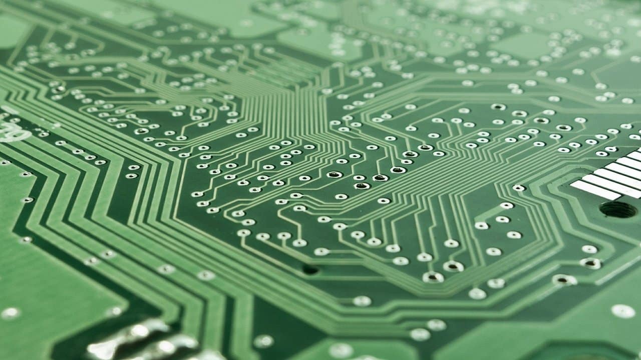
PCB boards are physical components of electronic devices. It is a board that has lines and pads that connect various points together.

Contents
1 What are PCB boards used for?
1.1 What are the advantages of PCB board?
2 What are PCB boards made of?
2.1 What is fr4 in PCB?
2.2 Why Copper is used in PCB?
3 What are the different types of PCB boards used?
4 What is PCB fabrication process?
4.1 What is lamination in PCB?
4.2 How to test a PCB board?
5 What is Gerber file in PCB?
5.1 What are the lines on a PCB board called?
5.2 What is PCB legend?
6 How much is a PCB board?
What are PCB boards used for?
PCB is used to mechanically support and electrically connect electronic components using conductive pathways, tracks or signal traces etched from copper sheets laminated onto a non-conductive substrate.
What are the advantages of PCB board?
When properly laid out, a PCB minimizes electronics noise that could significantly degrade performance. The electrical components on a PCB are organized in such as way that the path lengths of the electrical current between them are minimized, leading to low radiation and pickup of electromagnetic waves.What are PCB boards made of?
The substrate most commonly used in printed circuit boards is a glass fiber reinforced (fiberglass) epoxy resin with a copper foil bonded on to one or both sides. PCBs made from paper reinforced phenolic resin with a bonded copper foil are less expensive and are often used in household electrical devices.
What is fr4 in PCB?
FR-4 (or FR4) is a NEMA grade designation for glass-reinforced epoxy laminate material. FR-4 is a composite material composed of woven fiberglass cloth with an epoxy resin binder that is flame resistant (self-extinguishing).
Why Copper is used in PCB?
The most common element used to make traces is copper. Why is copper such a popular choice in the PCB industry? The number one benefit of copper is that it is highly conductive. This means that it can easily transmit signals without losing electricity along the way.
How many types of PCB boards are there?
Three ways are used for the construction of PCB called:
Single Sided PCBs.Double Sided PCBs.
Multilayer PCBs.
Most main boards have between 4 and 8 layers, but PCBs with almost 100 layers can be made.
It consists of substrate on which copper material is laminated to create a conduction path between different components. Required components are connected electrically with the PCB board using two different method named as through hole technology and surface mount technology.
What is PCB fabrication process?
PCB fabrication is the assembly method for circuit boards used in electronic and computer devices. The layers of the board are put together along with the specific surface pattern so it can be used in electronics manufacturing.
What is lamination in PCB?
Lamination is the process by which the core(s) of a PCB are melted together through heat and pressure with copper layers and prepreg layers (in multi-layer PCBs).
How to test a PCB board?
The PCB test of a board will use capacitance and resistance. A capacitance test will test for opens and shorts by sending a charge on the net (trace or plane) and then probe each net to measure the induced capacity. Resistance test measures resistance as the current flows through a conductor (trace), in ohms.
What is Gerber file in PCB?
The Gerber format is an open ASCII vector format for 2D binary images. It is the de facto standard used by PCB industry software to describe the printed circuit board images: copper layers, solder mask, legend, drill data, etc. Gerber is used in PCB fabrication data.
What are the lines on a PCB board called?
The electrical pathways or conductors are made up of two different parts. The first part is the lines themselves and they are called "traces". The second part is called a "land" or "pad". A land is a conductive surface providing a place on which to attach various components, make a connection or provide a test site.
What is PCB legend?
Legend or silkscreen or component identification, all terms that are used for the text layers and place on top of the solder mask layers.
How much is a PCB board?
PCB price of double sided for example,
Company: AiPCBASize: 100x100mm,
Color: Green
PCB thickness: 1.6mm
Price: $9.90/10pcs, $0.99 each
