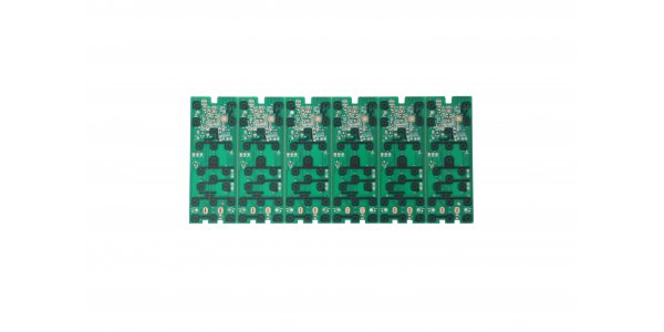
Electroless plating copper, also known as copper deposition or pore forming (PTH), is a self catalytic redox reaction. Firstly, an activator is used to adsorb a layer of active particles on the surface of the insulating substrate. Generally, palladium particles are used (palladium is a very expensive metal with high price and rising all the time. In order to reduce the cost, there are practical colloidal copper processes in operation abroad). Copper ions are first reduced on these active metal palladium particles, and these reduced metal copper crystal nuclei themselves It also acts as a catalytic layer for copper ions, which makes the reduction of copper continue on the surface of these new copper nuclei. Electroless copper plating has been widely used in PCB manufacturing industry.

At present, electroless copper plating is used to metallize PCB holes. The process flow of PCB hole metallization is as follows: Drilling → Deburring by grinding plate→ upper plate → whole hole cleaning treatment → double water washing → micro etching chemical roughening → double water washing → pre immersion treatment → colloidal palladium activation treatment → double water washing → degumming treatment (acceleration) → double water washing → copper deposition → double water washing → lower plate → upper plate → pickling → primary copper → water washing → lower plate → drying
1. Pretreatment of plating
1) Deburring
After drilling, some small burr will inevitably appear at the orifice of copper-clad mooring plate. If these burrs are not removed, the quality of metallized hole will be affected. The simplest deburring method is to polish the surface of the drilled copper foil with 200-400 water sandpaper. The mechanical deburring method is to use deburring machine. The grinding roller of deburring machine adopts nylon brush or felt containing silicon carbide abrasive. In general deburring machine, part of the burr is reversed to the inner wall of the orifice along the moving direction of the plate surface. The improved plate grinder has a bidirectional rotation with swing nylon brush roller, which eliminates this defect.

2) Clean the whole hole
There is a whole hole requirement for multi-layer PCB, the purpose is to remove drilling dirt and micro etching treatment. In the past, concentrated sulfuric acid was used to remove drilling pollution, but now alkaline potassium permanganate method is often used, followed by cleaning and adjusting treatment. In the process of hole metallization, electroless copper plating occurs simultaneously on the hole wall and the whole surface of copper foil. If some parts are not clean, it will affect the bonding strength between the electroless copper coating and the printed wire copper foil, so the substrate must be cleaned before electroless copper plating.
3) Copper clad foil roughening treatment
The chemical micro etching method is used to etch the copper surface (the etching depth is 2-3 μ m) to produce rough micro rough surface with active surface on the copper surface, so as to ensure the strong bonding strength between the electroless copper coating and the copper foil substrate. At present, sulfuric acid / hydrogen peroxide (H2SO4 / H202) is mostly used, the etching speed is relatively constant, and the roughening effect is uniform. Because hydrogen peroxide is easy to decompose, appropriate stabilizer should be added into the solution to control the rapid decomposition of hydrogen peroxide, improve the stability of etching solution and further reduce the cost.
If the etching rate without stabilizer is 100%, then the one with etching rate greater than 100% is positive accelerating stabilizer, and the one less than 100% is negative deceleration stabilizer. For the positive accelerating stabilizer, the etching speed is higher at room temperature (25 ° C) without heating. The negative deceleration stabilizer must be heated to produce the effect of micro etching copper. Attention should be paid to the newly opened micro etching solution. The etching rate is slow at the beginning of etching. 4G / L copper sulfate or 25% old solution can be added.
2、 Activation
The purpose of activation is to adsorb a layer of catalytic metal particles on the surface of the substrate, so that the whole surface of the substrate can be electroless copper plating reaction smoothly. The commonly used activation methods are sensitization activation method (step-by-step activation method) and colloidal solution activation method (one-step activation method).
1) Sensitization activation method
Firstly, sensitization.The commonly used sensitizer is stannous chloride aqueous solution.The sensitization treatment was carried out at room temperature for 3-5 min, and then activated after washing. Secondly, activation treatment.The commonly used ionic activation solution is palladium chloride solution.

The solution preparation and operation process of sensitization activation method is simple, and it has been widely used in the early hole metallization process of PCB. However, in the process of multi-layer bonding and pattern electroplating, this defect has become the main contradiction affecting the quality of printed circuit boards. Now, the chelating ion palladium step-by-step activation method is used to solve these problems, and it is less used now.
2) Colloidal palladium activation method (one-step activation method)
The loose catalytic layer formed on copper foil can be eliminated by using colloidal palladium activation solution. Moreover, the colloidal palladium activation solution has very good activity and obviously improves the quality of electroless copper plating layer. Therefore, it has been widely used in the hole metallization process of PCB.
-Preparation of colloidal palladium activation solution
a. Acid based colloidal palladium activation solution: 1g of palladium chloride was dissolved in a mixture of 100ml hydrochloric acid and 200ml pure water, and kept at 30 ℃ in a constant temperature water bath. While stirring, 2.54g of SnCl2 · 2H2O was added and stirred for 12 min. then, it was dissolved with the mixture of 60g SnCl2 · 2H2O, 200ml salt acid and 7g sodium stannate, and then was kept in a constant temperature water bath at 45 ℃ After heating for 3 h, the mixture can be diluted to 1 l with water.
b. Base colloidal palladium activation solution - weigh 0.25g palladium chloride, add 200ml deionized water and 10ml hydrochloric acid, stir at 30 ℃ to dissolve palladium chloride. Then add 3.2g stannous chloride and stir it properly, quickly pour it into the prepared mixed solution containing 50g urea, 250g sodium chloride, 0.5g sodium stannate and 800ml water, stir to make it completely dissolved, keep it at 45 ℃ for 3h, cool to room temperature, and dilute it to 1L with water.
-Colloidal palladium treatment process
Colloidal palladium activation solution was used as follows: Pretreatment → colloidal palladium activation → water washing → degumming → water washing → electroless copper plating

a. Pre-immersion treatment - if the roughened copper clad laminate is directly immersed in the colloidal palladium activation solution for activation after washing, the water content in the activation solution will increase continuously, resulting in premature aggregation of the colloidal palladium activation solution. Therefore, it is necessary to pretreat SN2 + in acidic solution for 1 ~ 2min before activation, and then directly immerse it in colloidal palladium activation solution for activation treatment. In preparation, hydrochloric acid should be mixed with water first, and then SnCl2 · 2H2O should be added to dissolve it by stirring, so as to prevent the hydrolysis of SnCl2.
b. Activation treatment - treat at room temperature for 3-5min. During the treatment, the copper clad laminate should be moved continuously to make the activation solution flow in the hole so as to form a uniform catalytic layer on the pore wall.
c. After degumming and activation, colloidal compounds with basic stannate around the palladium core are adsorbed on the surface of the substrate. Before electroless copper plating, the basic stannate should be removed to fully expose the active palladium crystal nucleus, so that the palladium crystal nucleus has very strong and uniform activity. After degumming and electroless copper plating, not only the activity of colloidal palladium is improved, but also the bonding strength between electroless copper coating and substrate is significantly improved. The commonly used solution is 5% sodium hydroxide solution or 1% Fluoroboric acid aqueous solution. The solution was treated at room temperature for 1 ~ 2min, and then electroless copper plating was carried out after washing.
