Altium designer software enhances electronic engineering workflows and reduces communication barriers between designers and manufacturers. It provides an easy-to-use, native 3D design-enhanced all-in-one design environment that includes all the tools designers need, such as schematics, circuit simulation signals, and complete analysis of PCB designs. The working environment can also be customized to meet the different needs of users. Altium Designer perfectly integrates technologies such as schematic design, circuit simulation, PCB drawing and editing, topology logic automatic layout, signal integrity analysis, and design output. It provides designers with a new design solution so that designers can easily design. The skilled use of Altium Designer will greatly improve the quality and efficiency of circuit design, which can effectively save overall costs and shorten the time to market.
AiPCBA is China's first online PCBA flexible intelligent manufacturing cloud platform, providing electronic product R&D companies with one-stop prototype production and volume production manufacturing services for BOM sourcing, PCB manufacturing, and SMT assembly.
Since 2016, AiPCBA has served nearly 100,000 customers around the world, providing them with one-stop services from product prototype manufacturing to volume production. We help customers to quickly produce and validate product prototypes and improve product defects. And we help customer to improve the speed of their product volume production and accelerate the process of product launch on the market. Learn more about AiPCBA’s PCB & PCBA manufacturing service.
How to generate Gerber files with Altium Designer?
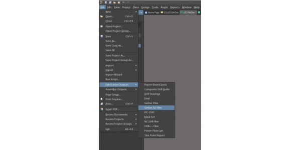
For customers using Altium Designer who is going to manufacture PCBs or PCBAs, this guide will help you configure and export Gerber files and NC Drill files in RS274X format. It is assumed that you have completed the design of the schematic and PCB layout. At this stage, you should have both a SchDoc file (schematic) and a PcbDoc file (PCB layout).step 1. Open Altium designer software, open the designed PCB file, in the PCB file environment, and left-click on file → fabrication, outputs → Gerber Files to enter the Gerber setup interface.
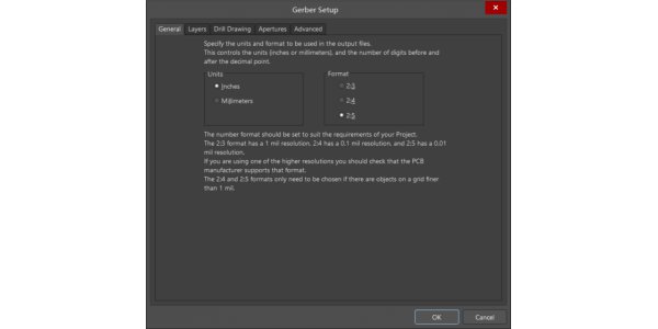
step 2. In the "General" option, select "inches" for "Units", and select 2:5 for Format, which has a relatively high dimensional accuracy.
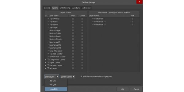
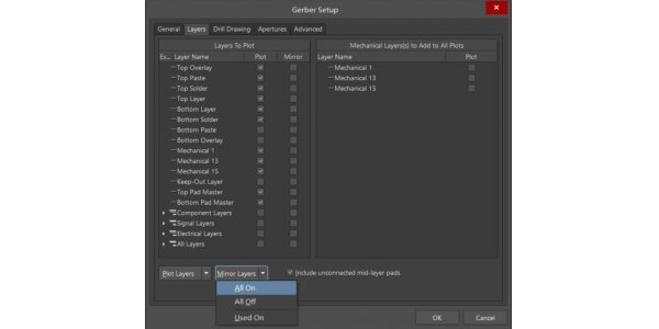
step 3. In "Layers", check "include unconnected mid-layer pads", select "used on" in the "Plot Layers" drop-down menu, check it out, and don't drop the layer. In the "mirror layers" drop-down "all off", do not select the mechanical layer on the right.
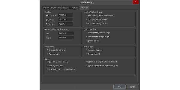
step 4. In "Apertures", tick √ to select "Embedded aperture (RS274X)" In "advanced", in the "Leading/Trailing Zeroes" area, select "Suppress leading zeroes", and click the "OK" button for the first output.
step 5. In the PCB file environment, go to file→fabrication outputs → Gerber Files again to enter the Gerber setup interface. In "layers", select all off in "plotlayer/mirrorlayers" on the left, and do not hit "include unconnected mid-layer pads" √, only the mechanical layer related to the outer frame of the board is selected.
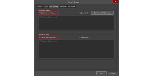
step 6. In "Drill Drawing", select the layer you want to export. Generally select "Plot all used layer pairs", "mirror plot" does not need to be selected. Make the same selections for Drill Drawing plots and Drill Guide Plots, and click the "OK" button for a second output.
step 8. Click the "OK" button to perform the third output. In the pop-up "import Drill Data" interface, left-click the "OK" button to output.
step 9. Pack and compress all the files in the Output file in the current project directory and send them to the PCB factory for processing.
AiPCBA Online 3D Gerber Viewer
After you generate Gerber files with Altium Designer, AiPCBA offers an online 3D Gerber Viewer for you to see your designs from a different perspective.AiPCBA has designed a free online 3D Gerber file viewer tool. With this viewer, you can upload a Gerber file and have a 360-degree view of your PCB design. Using the AiPCBA Online 3D Gerber viewer, you can check for errors, and use the zoom function to inspect the board. You don't have to be a registered user to take advantage of this useful tool, and you don't need a high-processing computer to operate.
PCB manufacturing in AiPCBA
AiPCBA focuses on not only 1-6 layers standard FR4 PCB boards but also specializes in 6-40 layers complex boards and flex, rigid-flex, Metal-core boards, etc.AiPCBA can produce the printed circuit boards with impedance control, HDI (High-Density Interconnection), Blind & buried board, thick copper board, gold finger, metal base PCB, ceramic substrate printed, and High-Frequency PCB, etc. As a mature, experienced, and versatile turnkey PCB manufacturer, AiPCBA has accepted orders for difficult printed circuit boards from all over the world. To this day, It is still well received.
You may be intersted
How to Generate Gerber File from DesignSpark?
How to Generate Gerber File from Kicad?