Introduction | What is a Multilayer Printed Circuit Board
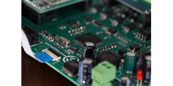
The double-sided board is a middle layer of dielectric, with both sides of the wiring layer, and the multilayer printed circuit board is a multilayer of wiring layers, with a dielectric layer between each two layers. The dielectric layer can be made very thin. A multilayer printed circuit board (Multilayer pcb) has at least three conductive layers, two of which are on the outer surface, and the remaining layer is synthesized in an insulating board. The electrical connection between them is usually achieved through plated through holes on the cross section of the circuit board.
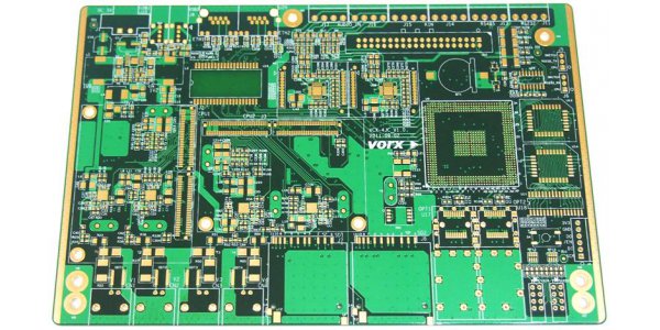
The circuit board determines the process difficulty and processing price according to the number of wiring surfaces. Ordinary circuit boards are divided into single-sided wiring and double-sided wiring, commonly known as single-sided and double-sided, but high-end electronic products are restricted by product space design factors. Outside the surface wiring, multiple layers of circuits can be stacked inside. During the production process, after each layer of circuits is made, they are positioned and pressed by optical equipment to allow the multilayer circuits to be stacked on a circuit board, commonly known as a multilayer printed circuit board. Any circuit board with two or more layers can be called a multilayer printed circuit board. Multi-layer printed circuit boards can be divided into multi-layer rigid circuit boards, multi-layer flexible and hard circuit boards, and multi-layer flexible-hard circuit boards.
Manufacturing Process | Multilayer Printed Circuit Board Generation Process
1.PCB Layout
The first step in PCB production is to organize and check the PCB layout.
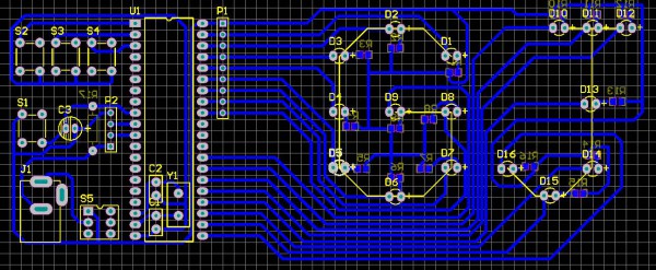
2.Core Board Production
Clean the copper clad board, if there is dust, it may cause short circuit or open circuit in the final circuit.3. Transfer of Inner PCB Layout
First, we need to make the two layers of the middle core board (Core). After the copper-clad board is cleaned, it will be covered with a photosensitive film.4. Core Board Drilling And Inspection
The core board has been successfully manufactured. Then punch holes in the core board to facilitate alignment with other materials.
5.Lamination
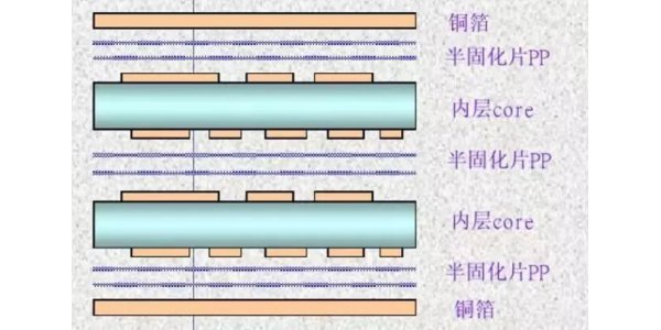
Here we need a new raw material called Prepreg, which is the adhesive between the core board and the core board (PCB layer number> 4), and the core board and the outer layer of copper foil, and also plays an insulating role.
6.Drilling
So how to connect the 4 layers of copper foil without contact in the PCB? First, drill up and down through holes to punch through the PCB, and then metalize the hole walls to conduct electricity.7. Chemical Precipitation of Copper on the Pore Wall
Since almost all PCB designs use different layers of wiring to connect vias, a good connection requires a 25 micron copper film on the hole wall.8. Transfer of outer PCB Layout
Next, the PCB layout of the outer layer is transferred to the copper foil. The process is similar to the principle of the previous PCB layout transfer of the inner core board. The photocopying film and photosensitive film are used to transfer the PCB layout to the copper foil. The positive film will be used for the board.9.Computer Control and Electroplated Copper
After the copper plating is completed, the computer also arranges to plate a thin layer of tin. After uninstalling the tin-plated PCB, check to ensure that the thickness of the plated copper and tin is correct.10.Etching of outer PCB
Next, a complete automated assembly line completes the etching process. First clean the cured photosensitive film on the PCB. Then remove the unnecessary copper foil covered with strong alkali. Then remove the tin plating layer on the copper foil of the PCB layout by using a de-soldering solution. After cleaning, the 4-layer PCB layout is complete.
Applications | Main Application areas of Multilayer Printed Circuit Boards
1. Consumer Electronics Products:
covers common products used by the general public. These products include daily-used smartphones, microwave ovens, and smart home appliances. Each of these products includes PCBs, but more and more manufacturers use them. Multilayer PCBs replace standard single layers. why? Most of the reasons are consumer trends. The use of multi-layer PCBs is conducive to increasing its functions and reducing product size, which is more in line with the compact and intelligent concept in the age of technology.
2. Computer Electronics:
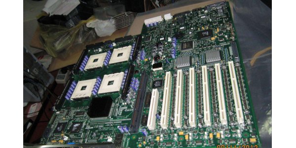
All products from servers to home computers use multilayer PCBs, mainly because they save space and have high performance. Among these products, high performance and low cost production are particularly important. Because of this, multilayer PCBs are the ideal solution for many technologies in the industry.
3. Automobiles:
In the modern era, automobiles are becoming more and more dependent on electronic components, especially with the rise of electric vehicles, from GPS and on-board computers to electronic control displays, various automotive parts, etc., the more correct components become More and more important.
4. Industrial:
Multilayer PCBs are indeed more durable than several other options on the market today, making them ideal for applications where rough handling may occur every day. As a result, multilayer PCBs have become popular in several industrial applications, the most noticeable of which is industrial control. From industrial computers to control systems, multilayer PCBs are widely used in manufacturing and industrial applications to run machinery, and are favored for their durability, small size, and functionality.
5. Medical equipment: Compared with single-layer alternatives, multilayer PCBs are particularly popular in the medical industry because of their small size, light weight, and powerful functions. These benefits have led to multilayer PCBs being used in modern medical equipment such as modern X-ray equipment, heart monitors, CAT scanning equipment, and medical test equipment.
6. Military And Defense:
Due to its durability, functionality, and lightness, multilayer PCBs can be used for high-speed circuits, which has become an increasingly important issue in military applications. Due to the trend of the defense industry towards highly compact engineering design, they are also favored because the compact multi-layer PCB leaves more space for other components to develop existing functions.
7. Telecommunications:
Telecommunications equipment often uses multilayer PCBs in many conventional applications, such as signal transmission, GPS and satellite applications. The reason is mainly its durability and functionality. PCBs for telecommunications applications are often used in mobile equipment or outdoor towers. In such applications, durability is essential while still maintaining a high level of functionality.
8. Aerospace:
As a high-tech field, every aerospace product must pursue high quality and high performance. The supporting equipment such as aircraft and rockets are very dependent on electronic equipment. These must be calculated with extreme accuracy. In this case, multilayer PCBs provide a suitable solution.
