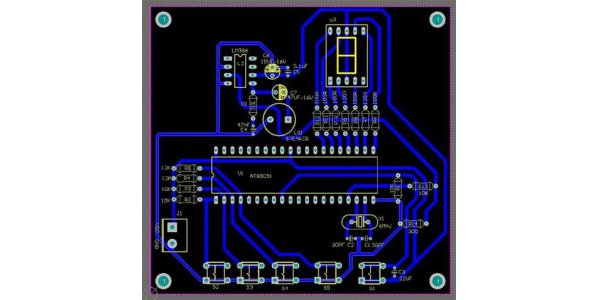
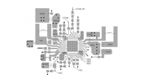
The basic design process of general PCB is as follows: preliminary preparation > PCB structure design > PCB layout > routing optimization and silk screen printing > network and DRC inspection and structure inspection > plate making.
1) Preliminary preparation
This includes the preparation of component libraries and schematic diagrams. To make a good board, we should not only design the principle, but also draw well. Before PCB design, it is necessary to prepare the component library of schematic PCB. Protel (PCB design software) can be used for component library.

2) PCB structure design
In this step, according to the determined PCB size and mechanical positioning, the PCB surface is drawn in the PCB design environment, and the required connectors, buttons / switches, screw holes, assembly holes, etc. are placed according to the positioning requirements. And fully consider and determine the wiring area and non wiring area (such as how much area around the screw hole belongs to the non wiring area). PCB design price is available on AiPCBA.
3) PCB layout
How are the principles of layout of components of PCB? The layout is to put devices on the board. At this time, if all the preparatory work mentioned above is done well, you can generate the network table (Design > create netlist) on the schematic diagram, and then import the network table (Design > Load nets) on the PCB diagram. You can see the whole stack of devices clattering up, and there are flying wires between the pins to indicate the connection. Then you can lay out the device. The general layout is divided into digital circuit area (i.e. fear of interference and interference), analog circuit area (fear of interference) and power drive area (interference source). Circuits for the same function should be placed as close as possible, and the components should be adjusted to ensure the most concise connection; at the same time, the relative position of each function block should be adjusted to make the connection between function blocks the most concise. For high-quality components, the installation position and strength should be considered; The heating element should be placed separately from the temperature sensitive element. If necessary, the thermal convection measures should be taken. The I / O driver should be close to the edge of the printed board and the lead-in connector. The clock generator (such as crystal oscillator or clock oscillator) should be as close as possible to the device using the clock A decoupling capacitor should be added between the power input pin of each integrated circuit and the ground (generally the single stone capacitor with good high frequency performance is used); when the circuit board space is relatively dense, a tantalum capacitor can be added around several integrated circuits. The discharge diode (1N4148) should be added to the relay coil. The layout should be balanced and orderly, and the top and bottom should not be heavy.

4) Wiring
Wiring is the most important process in the entire PCB design process. This will directly affect the performance of the PCB board. In the PCB design process, there are generally three such divisions of wiring: the first is routing, then the most basic requirements in PCB design. If none of the lines are routed then it will be an unqualified board. The second is the satisfaction of electrical performance. This is a measure of whether a printed circuit board is qualified. After wiring, carefully adjust the wiring so that it can achieve the best electrical performance. Then comes the beauty. If your wiring is laid, there is nothing to affect the performance of electrical appliances, but at first glance the messy past, plus the colorful, colorful, then how good your electrical performance, in the eyes of others is still a piece of garbage. This brings great inconvenience to testing and maintenance. The wiring should be neat and uniform, not crisscross and unruly. These must be achieved under the condition of ensuring the performance of electrical appliances and meeting other individual requirements, otherwise it will be a waste of money.
What is the Wiring Rules between Components?Under normal circumstances, the power cord and ground wire should be wired first to ensure the electrical performance of the circuit board. Within the scope of the conditions, try to widen the width of the power supply and the ground wire. It is better that the ground wire is wider than the power wire. Their relationship is: ground wire>power wire>signal wire, usually the signal wire width is: 0.2~0.3mm , and the thinnest width can reach 0.05~0.07mm, the power cord is generally 1.2~2.5mm. For the digital circuit PCB, a wide ground wire can be used to form a loop, that is, to form a ground network to use (analog circuit ground can not be used in this way). Designers need to pre-wiring the more strict lines (such as high-frequency lines), and the input and output side lines should avoid adjacent parallel to avoid reflection interference. Ground wire isolation should be added when necessary, and the wiring of two adjacent layers should be perpendicular to each other, and parasitic coupling is likely to occur in parallel.
5) Wiring optimization and screen printing
The time for optimizing wiring is twice the time for initial wiring. After confirming that there is nothing to be modified, you can lay copper (Place->polygon Plane). Copper laying generally lays ground wires (note the separation of analog ground and digital ground), and it may also need to lay power when multi-layer boards. For screen printing, be careful not to be blocked by the device or removed by vias and pads. At the same time, when designing, we should look squarely at the component surface, and the words on the bottom layer should be mirrored to avoid confusion.
6) Network and DRC inspection and structural inspection
Firstly, under the premise of confirming that the circuit schematic design is correct, the generated PCB network file and the schematic network file are subjected to a network check (NET CHECK) of the physical connection relationship, and the design is corrected in time according to the output file result to ensure the correctness of the wiring connection relationship. After the network check is passed correctly, the DRC check is performed on the PCB design, and the design is revised in time according to the output file that results to ensure the electrical performance of the PCB wiring. Finally, it is necessary to further check and confirm the mechanical installation structure of the PCB.
7) Plate making
Before plate making, it is better to have a review process. PCB design should be extremely careful, fully consider all factors (such as easy maintenance and inspection, many people do not consider it), and strive for excellence, so that we can definitely design a good printed circuit board.
