The well-designed circuit board needs to be made by the circuit board processing factory, and then after the proofing comes back, all kinds of components are welded on, and then they are assembled into the shell of the product to form a complete electronic product. So the circuit board proofing is an important link in the production process of electronic products. How about the customization process?

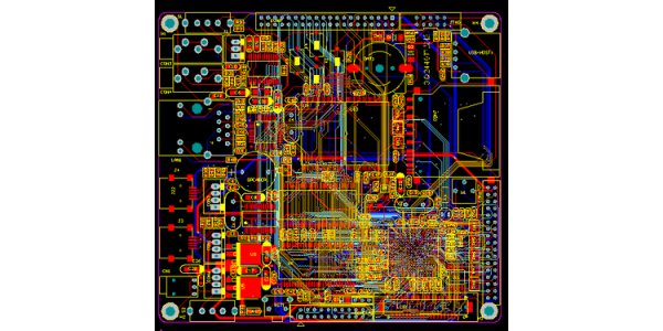
First of all, using Protel and other circuit design software on the computer, every Protel PCB designer needs to know PCBA concepts. Drawing the circuit schematic diagram and PCB (component package diagram). then put the heat transfer paper into the ordinary printer, adjust the appropriate printing ratio, and print the black and white PCB diagram. Next, the oxide layer on the surface of copper clad laminate is polished with sandpaper to make it look smooth and bright. Fix the heat transfer paper with printed PCB on the copper clad laminate polished in last step, and send it to the heat transfer machine (the common heating iron can also be used to replace the heat transfer machine) for printing, so that the toner containing the PCB diagram is printed on the copper clad laminate by hot pressing, and the heat transfer paper is gradually torn off.

Pour the corrosive solution into the plastic box, and then put the copper clad laminate with printed PCB pattern into the corrosive solution. After a period of corrosion (according to the different concentration of corrosive solution, the time is different), about half an hour to an hour (get access to know the way to clean a PCB of corrosion). Pour out the corrosive liquid, take out the corroded copper clad laminate, then use sandpaper to gently grind off the toner on the PCB on the CCL. The copper circuit routing on the PCB diagram will become exactly the same as that of the PCB pattern. Finally, put the obtained copper clad laminate into the drilling machine and drill holes one by one according to the positions of all holes in the PCB diagram, and then the components can be soldered up accordingly, and the whole PCB plate making process is finished.
By the way, some precautions of PCB proofing cannot be ignored. Firstly, pay attention to control the quantity of proofing. Because circuit board proofing is usually carried out in small batch production, the start-up cost of proofing manufacturers is high, which will increase the cost of enterprise proofing. Secondly, pay attention to the approval of proofing process. In addition to the process of proofing, the manufacturer should also pay attention to the process of proofing to meet the requirements of the manufacturer. Thirdly, pay attention to the layout of proofing signal. Whether the signal layout of the template is complete and reasonable will affect the quality of the whole proofing. Therefore, when proofing the circuit board, the enterprise should pay attention to the signal layout of the proofing to ensure that it is complete and reasonable, and should check the electrical aspects, so as to better improve the electrical performance and stability of the circuit board, and also reduce the noise.
