
1.0 PCB board design basics
PCB is a substrate for assembling electronic parts. Usually, there is a board with semiconductors, connectors, resistors, diodes, capacitors, radio equipment, and so on, and that board is a PCB. The following article will show the methods for designers how to place these electronic components on the board.2.0 Boards introduction
2.1 Single- Sided Boards (SSB)Generally, single-sided boards’ components and wires are concentrated on different panels. As only one side of the SSB can be wired, the wiring of the SSB cannot be crossed and just only be wired separately, which makes the SSB receive a lot of restrictions.
2.2 Double-Sided Boards
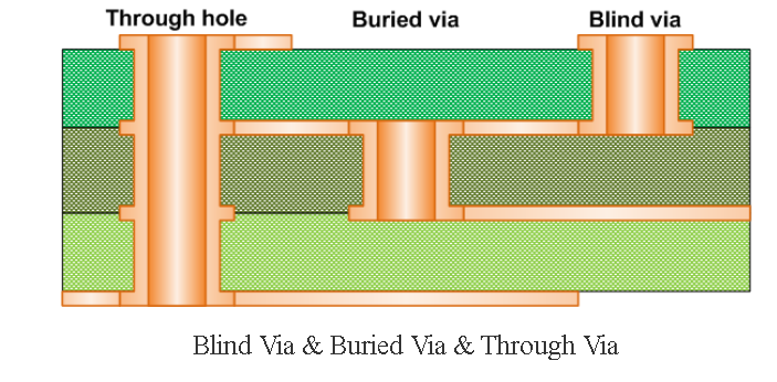
To ensure double panel wiring, via hole is a must on double-sided boards. The purpose of the via hole is to connect the two surface circuits. The advantage of this is that the two layers can be connected so that designers can cross over wire with each other on the PCB.
2.3 Multilayer Boards
To increase the area that can be wired, more single/double sided wiring boards are used.
Multilayer boards use multiple double panels, and a layer of insulation (Stitching) is placed between each panel. The number of layers represents the number of separate wiring layers.
The number of layers is usually an even number (including the two outermost layers). Most PCBs are 4-8 layers in structure.
3.0 PCB main components
3.1Copper Clad Laminate (CCL)CCL is made of wood pulp paper or glass fiber cloth as reinforcing material, impregnated with resin, single or double sides for copper clad, and then hot pressed.
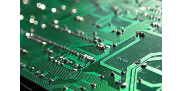
The substrate of PCB is made of an insulating, insulating, and non-bending copper-clad plate. The slim wiring material visible on the surface is copper foil. The copper foil was originally covered over the entire board but was partially etched during the manufacturing process. Therefore, what's left is a network of tiny lines.
Pads are used to make the welding with electrical connections elements and act as a fixator.

3.4 Via Hole
The Via hole is used to realize the electrical connection between different working layers, and the inner wall of the Via hole is also metallized.
Insulation layer on PCB to protect copper wire and prevent parts from being welded to incorrect locations.

To read PCB or assembly, debugging and other needs, designer can add some auxiliary information that including graphics or words.
4.0 Basic design process

The designer also needs to make the BOM when generating the schematic.
Designers need to put the schematic, bill of materials, hardware dimensions, layout files, assembly drawings, Gerber folders and component placement files all into the PCB document. If conditions permit, the designer can also design a user guide.
Designers need to make sure that their schematics contain enough detail.
According to the various properties of components to be placed, and before the wiring of the second check and adjustment.
The designer can maximize the area of heat transferred to the atmosphere so that the heat conduction plane distributes evenly in most situation. This method is effective in lowering the temperature.
Device placement sequence: Connectors - Power circuits - sensitive/precision circuits - key circuit components-other devices.
Designers must pay attention to all problems encountered in reviewing the PCB because they need to correct and correct the PCB based on the feedback generated by the review.
5.0
If you are not familiar with PCB design,
please refer to: The First Step of DFM: Reliability Design of PCB Layout. In
addition, there are several articles on PCB Design Layout Rules
Recommendations and PCB Design Guidelines – Heavy EXTREME Copper Board. These
articles are all explained in more detail. Alternatively, you can find more articles
on the AiPCBA Home Page, and these articles may be helpful to you.